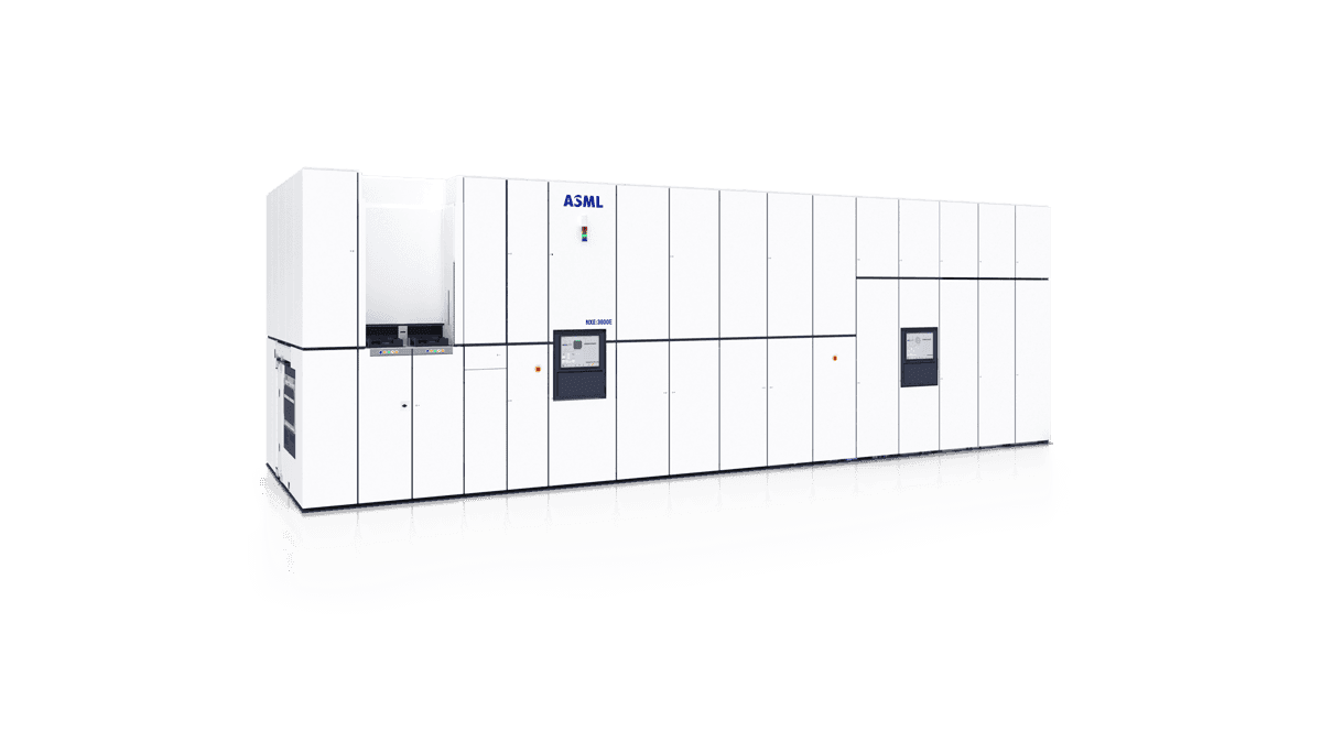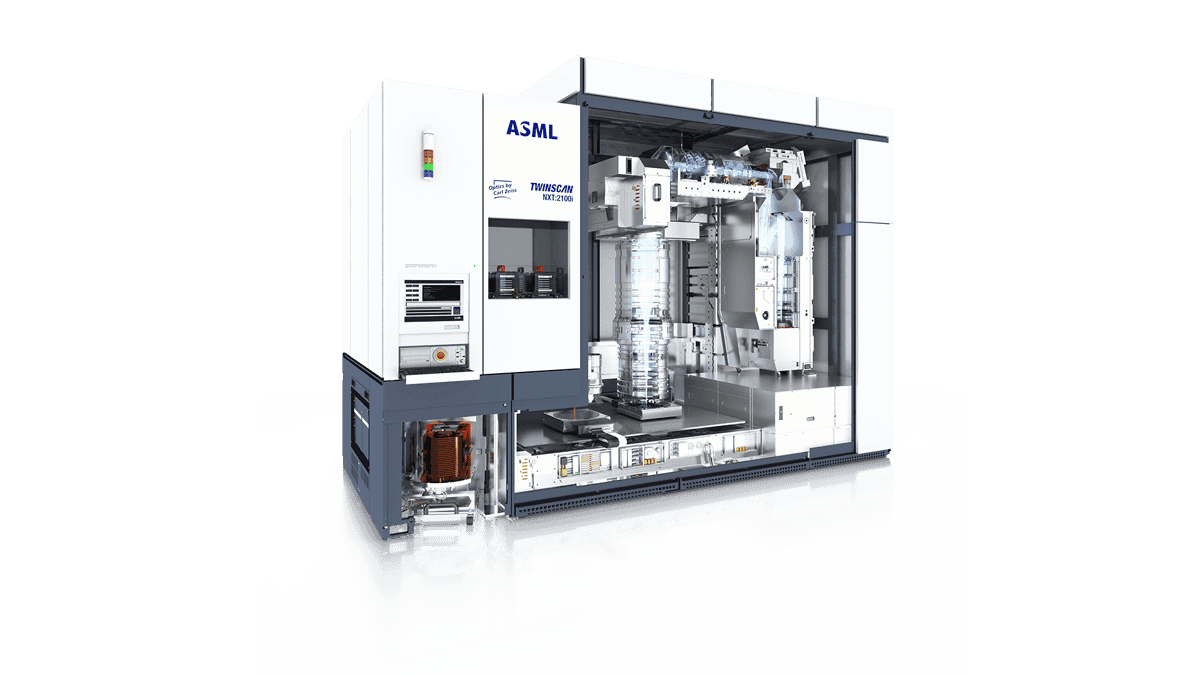
ASML

High-NA EUV (TWINSCAN EXE)

Active

The 0.55 NA anamorphic-optics scanners for sub-2nm chipmaking - at ~$380M each, the most expensive production tools ever built. The production-grade EXE:5200B installed at Intel in Q4 2025 for the 14A node; on July 15, 2026 select layers of Intel's Panther Lake (18A) chips became the first High-NA-patterned product to reach high-volume manufacturing. On September 8, 2026 Intel Foundry and ASML said more than one million wafers had been processed on High-NA tools across certification, R&D and those Panther Lake layers. As of Semicon Taiwan 2026, 10 EXE systems were running at four customers with three more shipping, July fleet availability was 84% (90% Q4 target), and the qualified EXE:5200B had reached 135 wafers per hour in acceptance testing. TSMC said on September 8, 2026 that it intends to use High-NA in high-volume manufacturing from 2030.

Latest update Sep 14, 2026
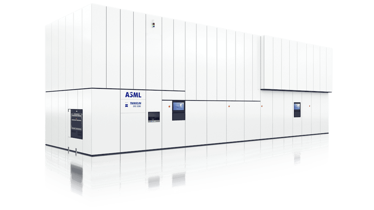
High-NA EUV (TWINSCAN EXE)

01

Current status

High-volume validation achieved via Intel Panther Lake (18A, Jul 2026); Intel Foundry and ASML reported more than one million High-NA wafers processed as of Sept 8, 2026 (certification, R&D and select production layers combined); Intel 14A risk production in 2027 is the next insertion; 10 systems live at 4 customers as of Semicon Taiwan 2026 with a 90% Q4 availability target; TSMC committed on September 8, 2026 to High-NA high-volume manufacturing from 2030, with a joint 12-inch photomask initiative (pilot 2031, production 2033); Reuters reported September 14 that Samsung and SK Hynix both set 2028 High-NA DRAM production, while Micron ordered tools without a date

02

Specifications3

Throughput (EXE:5200B)
135 wafers/hour in acceptance testing

(AB mode); roadmap 160 WPH on EXE:5200C, 175 on EXE:5200D, 180 on EXE:5400E, >250 on planned EXE:5600

System price
~$380M ($350-400M installed)
Fleet

10 systems running at 4 customers, plus 3 shipping or installing (Semicon Taiwan 2026)

03

Upcoming milestones2

Announced next steps from ASML that mention High-NA EUV (TWINSCAN EXE).

  1. 2027

    First High-NA production insertion: Intel 14A risk production

    Intel's 14A node is the first process natively built around High-NA EUV, with risk production slated for 2027 and high-volume manufacturing in 2027-2028. Intel already dual-qualified select Panther Lake (18A) layers on High-NA in July 2026 as an interim validation step; ASML plans 80-85 low-NA EUV systems for 2027 alongside the High-NA ramp. Re-verified September 2026: no change to the 14A timing, and Semicon Taiwan comments focused on EXE availability rather than a new Intel insertion date.

  2. 2028-2030

    Convert TSMC, Samsung and SK hynix High-NA commitments into high-volume layers

    TSMC said on September 8, 2026 that it intends to use High-NA EUV in high-volume manufacturing for advanced nodes from 2030, starting on 6-inch masks, and joined ASML in an industry initiative for 12-inch High-NA photomasks (pilot line 2031, production-ready 2033). The same day Samsung said it will put High-NA into DRAM high-volume manufacturing by 2028, an industry first, and joined the 12-inch mask initiative; Reuters reported on September 14 that SK hynix set the same 2028 DRAM date, while Micron has ordered tools without a production date. Intel Foundry and ASML said more than one million wafers have been processed on High-NA tools across certification, R&D and selected Panther Lake (18A) layers. The near-term demand test is whether those dated commitments turn into high-volume layers outside Intel's already-shipping Panther Lake High-NA use and the still-pending Intel 14A insertion. Semicon Taiwan 2026 said 10 EXE systems were already running at four customers, with three more shipping.

04

In the news2

  1. Samsung and SK Hynix set 2028 High-NA DRAM dates

    Reuters reported September 14 that Samsung and SK Hynix have both set 2028 dates to begin High-NA EUV DRAM production, while Micron has ordered tools without a production date. TSMC remains committed to High-NA high-volume manufacturing from 2030, and Intel has processed more than one million High-NA wafers across certification, R&D and select Panther Lake layers. ASML CEO Christophe Fouquet said the AI boom is not over and that memory makers are more aggressive on High-NA as low-NA EUV tools are all but sold out through 2027.

    Reuters

  2. ASML targets High-NA EUV production availability by year-end

    At Semicon Taiwan 2026, ASML High-NA product chief Greet Storms said the company expects 0.55-NA EXE systems to reach the availability customers need for high-volume manufacturing by the end of 2026, targeting 90% fleet availability in the fourth quarter after 84% in July. Ten High-NA systems are running at four customers, with three more shipping or installing, and EXE tools had accumulated more than 1.35 million wafer exposures by mid-July. The qualified EXE:5200B reached 135 wafers per hour in acceptance testing, with a longer-term availability goal of 93%.

    Bits & Chips TrendForce

05

More from ASML4

06

More in Semiconductors