Taiwan Semiconductor Manufacturing Company, founded in Hsinchu in 1987 by Morris Chang, invented the dedicated-foundry business model and now dominates it utterly: 69.9% of the global foundry market in 2025, holding 72.5% in Q2 2026 (TrendForce, published Sept 9-10), with Samsung a distant second at 5.9%.
It is effectively the sole manufacturer of leading-edge AI silicon - Nvidia, Apple, AMD, and Broadcom all fab their flagship chips there - which made it the primary beneficiary of the AI buildout: 2025 revenue hit a record $122.4B (+35.9%), and Q1 2026 revenue grew another 35.1% to $35.9B at a 66.2% gross margin. Q3 2026 revenue was NT$1,494.24 billion ($46.72 billion), with gross margin 66.4% and operating margin 58.7%. Wafer revenue was 2nm 8%, 3nm 33%, 5nm 28% and 7nm 10%, so 3nm overtook 5nm. Q4 guidance is revenue of $52.3-54.3 billion, gross margin 65-67% and operating margin 56.5-58.5%. On September 8, 2026 TSMC said it will put ASML High NA EUV into high-volume manufacturing from 2030. Its N2 (2nm) node, the company's first gate-all-around process, entered volume production on schedule in Q4 2025 at Fab 22 in Kaohsiung, with the enhanced N2P variant due in H2 2026 and the A16 node (backside power delivery) now slated for 2027 after slipping from late 2026. On Oct. 15, 2026 TSMC reiterated 2026 capex at $60-64 billion and said 2026-2028 spending will be significantly higher, while globalizing its footprint: Arizona's Fab 21 has produced 4nm chips at Taiwan-par yields since Q4 2024. On the Oct. 15 call Wei said the second Arizona fab is built and in tool move-in, with volume production in Q3 2027, slightly ahead of plan. He said teams are evaluating Texas and a customer Terafab that TSMC would have to run, with no decision and no named customer. He confirmed a GlobalFoundries back-end deal; GF's Oct. 8 release describes a five-year $2 billion Malta silicon-interposer agreement ramping in the first half of 2028, without a named CoWoS generation, unit volume, TSMC capex or Arizona packaging. On its July 16 call TSMC had pledged roughly $100 billion more for Arizona; Japan's JASM is building a second Kumamoto fab upgraded to 3nm, now targeted for 2028 after the upgrade pushed back its original late-2027 goal. On September 14, 2026 the Dresden ESMC joint venture held a topping-out ceremony, with president Christian Koitzsch saying construction is on schedule and the first process-equipment installation is due in the second half of 2027, with production still targeted for late 2027. TSMC is also diversifying beyond logic: on August 10, 2026, it announced a ~$6.3B joint venture with Sony (Sony 60%/TSMC 40%) to build a Kumamoto image-sensor fab targeting 2029 mass production. A January 2026 US-Taiwan trade deal exempts TSMC from new 25% Section 232 semiconductor tariffs in proportion to its US buildout. The overhang remains geopolitical: the vast majority of its leading-edge capacity sits on Taiwan, at the center of US-China tension.
The enhanced 2nm node enters volume production, offering a performance/power step over N2 for the 2027 flagship chip generation while N2 itself ramps through Taiwan's Fab 22 and Fab 20. TSMC's public 2nm page and later 2026 roadmap reporting still schedule N2P for the second half of 2026; no official start-of-volume announcement has been published as of September 11, 2026. Baseline N2 capacity remains headed toward about 100,000 wafers/month by year end.
TrendForce, citing Economic Daily News analysts on September 7, 2026, reported that TSMC's 3nm node is expected to overtake 5nm in revenue share for the first time in the second half of 2026, with third-quarter 3nm output value projected above NT$400 billion and more than 30% of total revenue. TSMC's own second-quarter mix was 5nm at 33% and 3nm at 30% (up from 25% in Q1). The mid-October Q3 print is the first official check of whether that crossover has begun.
MediaTek said on September 15, 2026 that Dimensity 9600 Pro is its first smartphone processor built on TSMC's 2-nanometer process, with a companion Dimensity 9600M on TSMC 3nm for a broader flagship segment, and that the first phones using both chips are expected this quarter. Reuters reported the NPU delivers a 51 percent improvement versus the prior generation in processing a user's prompt before a model starts generating a response. Watch whether named Xiaomi, Oppo, or Vivo models actually ship on N2 before year-end, which would be the first public consumer proof of TSMC 2nm volume beyond HPC wafers.
TSMC's newly finalized base wafer-price increases of 5-10% across advanced nodes (plus a 10-15% surcharge on incremental HPC orders) and its first mature-node price hike in three-plus years take effect, testing how much pricing power TSMC's near-monopoly on leading-edge capacity gives it against Apple, Nvidia, AMD, and Qualcomm. No public revision as of September 17, 2026.
TSMC's first node with Super Power Rail backside power delivery enters volume production, now targeted for 2027 after the April 2026 roadmap update moved it from H2 2026. TSMC confirmed in August 2026 that development and verification are complete and that initial Q4 2026 production is on track, but broad-based volume production tied to customer qualification remains a 2027 event. TSMC's homepage still features A16 with Super Power Rail as the HPC/AI backside-power node. Watch whether AI/HPC lead customers land on schedule.
Meet near-doubled chipmaking-tool demand across ~20 simultaneous fab builds
TargetOngoing through 2027
Deputy co-COO Cliff Hou said at a Semicon Taiwan fireside chat, reported by Bloomberg on September 2, 2026, that TSMC's own estimate of quarterly equipment purchases has risen to about 1.9x what it projected in December 2025, as AI chip demand keeps outrunning capacity plans. TSMC is simultaneously constructing nearly 20 wafer fabs (13 in Taiwan, 5-6 overseas) - four to five times its normal construction pace - and flagged a shortage of experienced construction workers in Taiwan as a growing constraint on how fast that capacity can come online.
The most advanced node yet manufactured in the US: construction finished months ahead of schedule, equipment move-in starts Q3 2026, pilot 3nm production is targeted for early 2027, and volume N3 production for Q3 2027 (also described as the second half of 2027 in TSMC's 2025 annual report) - pulled in roughly a year from the original plan. No public confirmation as of September 17, 2026 that Phase 2 tools have finished move-in; Q3 2026 still has two weeks remaining.
TSMC's €10B+ European joint venture with Bosch, Infineon, and NXP (TSMC 70%) held a topping-out ceremony on September 14, 2026, 25 months after groundbreaking. ESMC president Christian Koitzsch said construction is on schedule and within budget, with about 2,000 workers on site. He put the next milestone - first manufacturing-process equipment installation - in the second half of 2027, after cleanroom interiors, the automated material-handling system, and power and water work are finished (earlier reporting had pointed to equipment move-in in H2 2026). Production of 28/22nm and 16/12nm automotive-class chips remains targeted for late 2027 at about 40k wafers/month.
Japan's second TSMC fab, under construction since October 2025, was upgraded in February 2026 from the originally planned 6/7nm to 3nm, confirmed by CEO C.C. Wei and approved by Taiwan's government in March 2026 - Japan's first leading-edge node. The upgrade raised the investment from ~$13.9B to ~$17B and set planned capacity at 15,000 12-inch wafers/month; equipment installation and mass production are now targeted for 2028, later than the pre-upgrade late-2027 goal. No newer official date as of September 17, 2026.
Complete a Taiwan CPO silicon photonics supply chain
After the Ministry of Economic Affairs' September 6, 2026 Semicon Taiwan statement, the near-term test is whether TSMC, ASE, MediaTek, Foxconn and the rest of the ~30-firm group can turn CPO from a foundry/OSAT capability into a fully domestic silicon photonics chain. Separately, Taiwanese media cited by Herald Business say TSMC is targeting CoPoS mass production in the second half of 2028 as a panel-level successor to sold-out CoWoS.
Sony-TSMC image sensor joint venture begins production
Sony Semiconductor Solutions and TSMC signed a definitive agreement on August 11, 2026 establishing Advanced Vision Semiconductor Manufacturing Corporation in Koshi City, Kumamoto - Sony contributing about JPY465B and TSMC about JPY282B in phases, consistent with the 60%/40% split first announced August 10. The JV will co-develop and manufacture next-generation image sensors, initially targeting high-performance camera sensors for smartphones (including Apple's iPhone) with longer-term ambitions in robotics and vehicle AI object recognition. Mass production is targeted for 2029 - TSMC's first move into image sensors. No newer official date as of September 17, 2026.
TSMC said on September 8, 2026 that it intends to use ASML High NA EUV in high-volume manufacturing for advanced nodes starting in 2030, with High NA layer counts expected to rise as AI transistor architectures get more complex. Near-term High NA production will use today's 6-inch photomasks; the 12-inch mask transition is a later productivity step.
Longtan Phase 3 Executive Yuan approval and first A14-class fab
After the NDC cleared a 104-hectare Longtan Science Park expansion on September 17, 2026, the plan still needs Executive Yuan approval, environmental assessment and non-urban land permits targeted through 2028, then park infrastructure from 2030. United Daily News, citing TSMC's supply chain, said TSMC plans three angstrom-era fabs there for A14 and below, with the first aimed for around 2030. Taoyuan Mayor Chang San-cheng said the city would handle land, resettlement, water and power.
With ASML, TSMC is leading an industry initiative to move High NA EUV photomasks from 6-inch to 12-inch format, targeting a 12-inch mask pilot line by 2031 to raise scanner productivity, lower chipmaking costs and remove stitching constraints. Full 12-inch High NA lithography systems are aimed at advanced-node production by 2033.
TSMC's investor calendar lists September 2026 monthly sales for October 8, 2026, the first official check after the August NT$514.806B record, then a mid-October quarterly report. Guidance (issued Jul 16, 2026) remains revenue of $44.6-45.8B (+37% YoY at midpoint, +12% QoQ), gross margin of 65-67%, and operating margin of 56-58%, as the N2 ramp and overseas-fab dilution weigh on margins. Watch whether 3nm overtakes 5nm as the largest revenue node (Q2 mix: 3nm 30%, 5nm 33%), whether 2nm capacity reaches the ~100,000 wafers/month year-end target, whether MediaTek's first 2nm phones are reflected as N2 volume, and whether the September 8 High NA 2030 commitment is repeated on the call.
On Oct. 15, 2026 TSMC reported third-quarter consolidated revenue of NT$1,494.24 billion, or $46.72 billion, net income of NT$763.06 billion and diluted EPS of NT$29.43, or $4.60 per ADR. Revenue rose 50.9% from a year earlier and 17.6% from the second quarter. Gross margin was 66.4% and operating margin was 58.7%, above the company's 58% guidance ceiling. 2-nanometer chips were 8% of wafer revenue and 3-nanometer chips 33%.
On Oct. 8, 2026 GlobalFoundries announced a manufacturing agreement with TSMC under which GF will supply silicon interposers for TSMC's CoWoS advanced-packaging ecosystem from its Malta, New York, fab. GF called the arrangement a multi-year $2 billion agreement with an initial five-year term and said volume production is expected to ramp in the first half of 2028, establishing a U.S. source of silicon interposers including embedded deep-trench-capacitor parts. Planned wafer volumes and a matching TSMC newsroom confirmation were not in the pages opened for this check.
TSMC said October 8 that September consolidated revenue was about NT$511.86 billion, down 0.6% from August and up 54.6% from September 2025. January through September revenue was NT$3,898.73 billion, up 41.1% year on year. Official July, August and September monthly tables sum to NT$1.494 trillion for the third quarter; TSMC's full Q3 results, margins and node mix remain scheduled for October 15.
Elon Musk said on Oct. 7 that Tesla and SpaceX will build and run the planned Terafab AI chip complex in Texas, writing that TSMC might sublease part of the site but nothing more than that. Reuters reported the posts after Musk called weekend TSMC talks just discussions. Intel CEO Lip-Bu Tan told Bloomberg the same day that Intel remains involved as a partner on the project, which is planned around Intel's 14A process. TSMC and Intel did not immediately comment to Reuters. A TSMC sublease is not a signed agreement.
Taiwan's National Development Council on September 17 approved a plan to expand Hsinchu Science Park's Longtan site by about 104 hectares, with NT$95.63 billion of park development funding, about 4,500 jobs, and a report still due to the Executive Yuan for final approval. United Daily News, citing TSMC's supply chain, said TSMC plans to return with three angstrom-era wafer fabs targeting A14 and below, with the first aimed for completion around 2030 and total investment estimated above NT$1 trillion if all three are built. Environmental review and non-urban land permits are scheduled through 2028, with park infrastructure construction from 2030.
MediaTek said on September 15 its Dimensity 9600 Pro is its first smartphone processor built on TSMC's 2-nanometer process, with a companion Dimensity 9600M on TSMC's 3-nanometer node for a broader flagship segment. Reuters reported the NPU delivers a 51% improvement versus the prior generation in processing a user's prompt before a model starts generating a response. MediaTek's own release said the first phones using the two chips are expected this quarter.
TSMC posted August 2026 net sales of NT$514.806 billion, up 53.3% from a year earlier and 10.1% from July, a fourth straight monthly rise as AI accelerators keep filling advanced-node capacity. January-August cumulative revenue reached NT$3.387 trillion, up 39.3% year over year. CNBC put the August print at about US$16.35 billion.
TSMC and ASML said on September 8, 2026 that TSMC intends to use High NA EUV in high-volume manufacturing for advanced nodes starting in 2030, with the number of High NA layers expected to rise as AI transistor architectures get more complex. The companies also launched an industry initiative to move High NA photomasks from today's 6-inch format to 12-inch, targeting a pilot line by 2031 and production-ready systems by 2033. CNBC reported that Samsung separately plans to use High NA for DRAM from 2028, joining Intel, which is already patterning some high-volume layers with the tools.
Taiwan's Ministry of Economic Affairs said on September 6, 2026 that TSMC, ASE, MediaTek, Foxconn and about 30 other Taiwanese companies are working to complete a domestic silicon photonics supply chain for co-packaged optics, a theme that dominated Semicon Taiwan 2026 in Taipei. The ministry said moving chip-to-chip links from copper to light can cut power use by 30 to 50 percent and is meant to keep CPO design, manufacturing and packaging on the island. Herald Business, citing Taiwanese media, separately reported TSMC is targeting mass production of next-generation CoPoS packaging in the second half of 2028.
TrendForce, citing Taiwan Economic Daily News analysts, reported on September 7, 2026 that TSMC's 3nm node is expected to overtake 5nm in revenue share for the first time in the second half of 2026, with third-quarter 3nm output value projected above NT$400 billion and more than 30% of total revenue. TSMC's own second-quarter figures showed 5nm at 33% of sales and 3nm at 30%, up from 25% in the first quarter. Wedbush, also cited in the report, expects monthly 3nm wafer starts to rise from 150,000 in the first half to 180,000 in early fourth quarter.
TSMC's need for chipmaking equipment has risen to about 1.9 times what it had projected in December 2025, deputy co-COO Cliff Hou said at a Semicon Taiwan fireside chat reported by Bloomberg on September 2, 2026, as the company races to keep pace with AI chip demand. TSMC is simultaneously constructing nearly 20 wafer fabrication plants, thirteen in Taiwan and five to six spread overseas, a pace it said is four to five times its normal construction rate, while flagging a shortage of experienced construction workers in Taiwan as a growing constraint on the buildout.
Sony Semiconductor Solutions and TSMC signed a legally binding definitive agreement on August 11 to form Advanced Vision Semiconductor Manufacturing Corp, a roughly $6.3 billion joint venture (Sony 60%, TSMC 40%) based in Kumamoto, Japan to develop and produce next-generation image sensors, targeting volume production in 2029. Sony will hold the controlling stake and contribute its Kumamoto chip factory alongside core sensor technology, product planning and design, while TSMC supplies its advanced process technology and manufacturing expertise.
TSMC's wholly owned Arizona subsidiary reported NT$36.07 billion (roughly $1.1 billion) in profit for the first half of 2026, up about 663% year over year and already exceeding its full-year 2025 profit, driven by tight advanced-node capacity and higher foundry pricing. TSMC's Japan subsidiary JASM also swung to profit in 2026, posting its first profitable stretch since Kumamoto production began in late 2024.
TSMC's board approved about $29.44 billion in capital appropriations for advanced-technology, packaging and fab construction at a meeting concluding August 11, and executed a legally binding definitive agreement with Sony Semiconductor Solutions to build the previously announced Kumamoto image-sensor joint venture. Sony will contribute about 465 billion yen and TSMC about 282 billion yen to the venture, which keeps its 60%/40% split and targets volume production of next-generation image sensors in 2029.
TSMC reported July 2026 revenue of NT$467.58 billion (about $16.03 billion) in an August 10 disclosure, up 44.7% year-on-year and 5.6% from June. Cumulative January-July revenue reached NT$2,872.06 billion, up 37% from the same period in 2025, as the company reaffirmed guidance for 2026 revenue growth above 40% in dollar terms on continued AI chip demand.
(TrendForce, reported Sept 9-10, 2026), up from 72.3% in Q1, with Samsung a distant second at 5.9% (down from 6.5%). Different research firms' foundry-share figures vary by methodology (Counterpoint had earlier put Q2 near 73%/Samsung 7%; TrendForce put FY2025 at 69.9%)
Latest quarterly revenue
NT$1,494.24 billion / $46.72 billion
(Q3 2026). Revenue +50.9% YoY and +17.6% QoQ in NT$; +41.2% YoY and +16.2% QoQ in USD. Net income NT$763.06 billion. Diluted EPS NT$29.43 ($4.60 per ADR).
Jan-Aug 2026 cumulative revenue
NT$3,386.87B
(+39.3% YoY); August alone NT$514.806B / ~US$16.35B (+53.3% YoY, +10.1% MoM), a fourth straight monthly rise and a new monthly record on AI chip demand
Market cap
~$2.22T as of September 10, 2026
(MarketBeat), recovering from the ~$1.97T late-August pullback; other September prints cluster around $2.22-2.28T depending on the TSM ADR close
2026 capex guidance
$60-64 billion, reiterated on the Oct
15, 2026 call. Management also said 2026-2028 capex will be significantly higher than the prior three years. No 2027 dollar budget was given.
2027 wafer price increase
Base prices to rise 5-10% across advanced nodes (5nm/4nm/3nm) from Jan 2027, plus a 10-15% surcharge on incremental HPC orders (up to ~25% combined); also TSMC's first mature-node (12/16/28nm) price increase in over three years. No public revision as of September 11, 2026.
Q3 2026 revenue guidance
July 16 guide was $44.6-45.8 billion, gross margin 65-67% and operating margin 56-58%. Oct. 15 actual was $46.72 billion, gross margin 66.4% and operating margin 58.7%.
Gross margin
66.4% in Q3 2026
(operating margin 58.7%, net margin 51.1%), down from 67.7% in Q2. Q4 gross margin guided to 65-67% and operating margin to 56.5-58.5%.
Advanced-node share of wafer revenue
79% from 7nm and more advanced nodes in Q3 2026: 2nm 8%, 3nm 33%, 5nm 28%, 7nm 10%. 3nm overtook 5nm.
Fabs
18
(incl. six 12-inch GIGAFABs); >17M 12-inch-equivalent wafers/yr. Still the 2025 annual-report count as of September 11, 2026; no newer official fab census published.
Customers / products (2025)
534 customers, 12,682 distinct products
Still the 2025 annual-report count as of September 11, 2026.
Arizona subsidiary H1 2026 profit
NT$36.07B
(~$1.1B), up ~663% YoY and already above full-year 2025 profit; Japan subsidiary JASM also swung to profit in 2026, its first profitable stretch since Kumamoto production began in late 2024. No newer Arizona subsidiary print as of September 11, 2026.
Market cap
About $2.38T
CNBC; TSM previous close $456.19, 5.19B shares outstanding
First TSMC 2nm smartphone SKUs
vivo X500 Pro Max on sale 24 Sept 2026 and X500 Pro on sale 29 Sept 2026 (Dimensity 9600 Pro, 2nm)
Market cap
About $2.45T
CNBC; TSM 7 Oct close $472.20, 5.19B shares
2nm wafer-revenue share
8% of Q3 2026 wafer revenue, up from 3% in Q2
September 2026 consolidated revenue
NT$511.86 billion, -0.6% MoM, +54.6% YoY
Jan-Sep NT$3,898.73 billion, +41.1%; Q3 monthly sum NT$1.494 trillion
Oct. 15, 2026 earnings release: Q3 revenue NT$1,494.24 billion ($46.72 billion), net income NT$763.06 billion, diluted EPS NT$29.43 ($4.60 per ADR). Gross margin 66.4%, operating margin 58.7%, net margin 51.1%. Wafer mix: 2nm 8%, 3nm 33%, 5nm 28%, 7nm 10%. Q4 guide: revenue $52.3-54.3 billion, gross margin 65-67%, operating margin 56.5-58.5%, at NT$31.8 per dollar. 2026 capex was reiterated at $60-64 billion; 2026-2028 spending was described as significantly higher, with no 2027 dollar figure. Arizona's second fab is built and tools are moving in; volume production is Q3 2027, slightly ahead of the prior schedule. Wei said Texas is under evaluation and a customer Terafab discussion continues, with any fab to be run by TSMC; no site decision and no named customer. He confirmed a GlobalFoundries back-end deal. GF's Oct. 8 release adds a five-year $2 billion Malta silicon-interposer agreement for CoWoS, with a ramp in the first half of 2028, and does not name a generation, unit volume, TSMC capex, or Arizona packaging. The Oct. 8 monthly sales print stays separate from this earnings release.
Revenue streams
High-performance computing (AI accelerators & data center)
Fabricating GPUs, AI accelerators, and server CPUs for Nvidia, AMD, Broadcom, and hyperscaler custom-silicon programs - 66% of Q2 2026 revenue and up 20% quarter-over-quarter, the dominant and fastest-growing stream, now two-thirds of the company.
Smartphone SoCs
Application processors and modems for Apple and other handset makers - 22% of Q2 2026 revenue (down 4% sequentially), historically TSMC's largest segment before AI overtook it.
IoT, automotive & consumer electronics
Specialty and mature-node chips for IoT devices (5% of Q2 2026 revenue), automotive (4%), and digital consumer electronics (1%), largely from 8-inch fabs and the Japan/China sites.
Advanced packaging (CoWoS / SoIC)
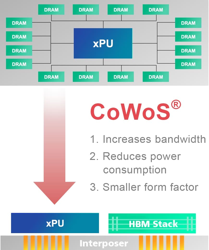
2.5D/3D packaging that assembles GPU dies with high-bandwidth memory - the binding constraint on AI accelerator supply. Capacity is being quadrupled toward ~130-140k wafers/month by late 2026, absorbing 10–20% of the 2026 capital budget; TSMC began outsourcing part of the process to OSAT partners in August 2026 to ease the bottleneck.
07
Track record
How past announced dates turned out.
2/4announced dates hit on time
2 Hit
2 Slipped
0 Missed
Hit
Confirm whether Q3 2nm wafer revenue moves past the Q2 3% start
Target October 8 and 15, 2026 · Resolved Oct 15, 2026
Q3 2nm wafer revenue was 8% of the total, up from 3% in Q2, per the Oct. 15, 2026 earnings release.
Announced in April 2024 for production in 2026, A16 was pushed to 2027 in the roadmap TSMC presented at its April 2026 North America Technology Symposium - the company's most visible recent node slip.
N2 entered volume production in Q4 2025 exactly as promised, confirmed December 30, 2025 - TSMC's first gate-all-around node, ramping at Fab 22 Kaohsiung and Fab 20 Hsinchu with reported yields around 70%.
Start construction of Kumamoto Fab 2 by end of 2024
Target End of 2024 · Resolved Oct 28, 2025
Construction was promised for end-2024 but began only in late October 2025, roughly ten months late, after local traffic and infrastructure concerns; the end-2027 operations target was retained and the planned process later upgraded to 3nm.
Q3 results, Q4 guide, Texas evaluation and GlobalFoundries confirmation
On Oct. 15, 2026 TSMC reported Q3 revenue of NT$1,494.24 billion ($46.72 billion), gross margin 66.4% and operating margin 58.7%. 2nm was 8% of wafer revenue, 3nm 33% and 5nm 28%. Q4 revenue was guided to $52.3-54.3 billion, with gross margin 65-67% and operating margin 56.5-58.5%. 2026 capex was reiterated at $60-64 billion. C.C. Wei said Arizona's second fab is built and taking tools, with volume production in Q3 2027, slightly ahead of plan. He said teams are evaluating Texas and talks continue on a customer Terafab that TSMC would have to run; no decision. He confirmed TSMC designed a GlobalFoundries back-end deal, without volumes, generations, TSMC capex or an Arizona packaging scope. GlobalFoundries' Oct. 8 release describes a five-year, $2 billion Malta interposer agreement with a volume ramp in the first half of 2028.
Q3 profit of NT$763.06 billion
On Oct. 15, 2026 TSMC reported Q3 consolidated revenue of NT$1,494.24 billion ($46.72 billion), net income of NT$763.06 billion and diluted EPS of NT$29.43 ($4.60 per ADR). Revenue rose 50.9% year on year. Gross margin was 66.4% and operating margin 58.7%. 2nm was 8% of wafer revenue and 3nm 33%.
Books Malta CoWoS interposers from GlobalFoundries
On Oct. 8, 2026 GlobalFoundries announced a manufacturing agreement with TSMC to supply silicon interposers for TSMC's CoWoS advanced-packaging ecosystem from GF's Malta, New York, fab. GF described a multi-year $2 billion agreement with a five-year initial term and said volume production is expected to ramp in the first half of 2028. Planned volumes and a TSMC newsroom confirmation were not disclosed in the pages opened.
Reports September 2026 sales of NT$511.86 billion
TSMC's 8 Oct English release and PDF table put September consolidated revenue at NT$511,857 million, down 0.6% from August's NT$514,806 million and up 54.6% from September 2025. January-September revenue was NT$3,898,727 million, up 41.1%. Official monthly figures for July (NT$467,580 million), August and September sum to NT$1,494,243 million for Q3. The IR monthly HTML table still left September blank at fetch. Full Q3 results, margins and node mix remain due 15 Oct after a 5-14 Oct quiet period.
TSMC offers no comment on Bloomberg Texas campus report
Bloomberg reported on 1 Oct 2026, citing unnamed people, that TSMC was weighing a multibillion-dollar Texas campus beyond its about $265B Arizona commitment, with each plant at least $20B and plans still early-stage. In a text message TSMC said it had no comment on market rumors. That is neither a confirmation nor a factual denial of a Texas site.
Musk says Tesla and SpaceX will run Terafab; TSMC at most a sublease
On 7 Oct 2026 Musk wrote that Tesla and SpaceX will build and run the planned Texas Terafab AI chip complex, adding that TSMC might sublease part of the site but nothing more. Reuters reported the posts and said TSMC did not immediately comment. This is not a TSMC operator role and is not a signed sublease.
First named TSMC 2nm phones go on sale in China
vivo said on 21 Sept 2026 that X500 Pro and X500 Pro Max globally debut Blue Crystal x Dimensity 9600 Pro, MediaTek's first 2nm flagship. Official China sale dates: X500 and X500 Pro Max on 24 Sept, X500 Pro on 29 Sept from 6,499 yuan. vivo's spec page lists CPU as Dimensity 9600 Pro on a 2nm process. GSMArena marks X500 Pro Available, released 29 Sept. MediaTek's own 15 Sept English release still does not name an OEM or SKU. TSMC has not printed September sales (due 8 Oct) or Q3 node mix (due 15 Oct), so 2nm remains 3% of Q2 wafer revenue until those reports.
NDC approves Longtan Phase 3 park expansion for A14-class fabs
Taiwan's National Development Council on September 17, 2026 approved the third-phase expansion of Hsinchu Science Park's Longtan site by about 104 hectares, with NT$95.63 billion of park development funding, about 4,500 jobs, and a report still due to the Executive Yuan for final approval. United Daily News, citing TSMC's supply chain, said TSMC plans to return with three angstrom-era wafer fabs targeting A14 and below, with the first aimed for completion around 2030 and total investment estimated above NT$1 trillion if all three are built. Environmental review and non-urban land permits are scheduled through 2028, with park infrastructure construction from 2030.
2026
Dresden ESMC fab tops out; first tools targeted for H2 2027
On September 14, 2026 European Semiconductor Manufacturing Company held a topping-out ceremony at its Dresden fab, 25 months after groundbreaking. President Christian Koitzsch said about 2,000 workers from 106 countries are on site, construction is on schedule and within budget, and the next milestone is installing the first manufacturing process equipment in the second half of 2027, after cleanroom interiors, the automated material-handling system, and power and water infrastructure are finished. Production of 28/22nm planar CMOS and 16/12nm FinFET automotive-class chips remains targeted for late 2027 at about 40,000 300mm wafers a month. The joint venture is TSMC 70% with Bosch, Infineon and NXP at 10% each, a roughly 10 billion euro project with about 5 billion euros of German state support.
China weighs export controls that would bar TSMC from Chinese-designed chips
China's Ministry of Commerce is reported, as of mid-August 2026, to be soliciting industry feedback on export controls covering advanced AI models, training data, and foreign chipmaking access - including a measure that would bar overseas foundries like TSMC from manufacturing advanced processors based on designs from Chinese companies such as Alibaba, ByteDance, and Huawei. The proposal, not yet enacted, would mirror US-led export controls in reverse and adds a new geopolitical risk vector alongside existing US Section 232 tariff exposure.
A16 development and verification completed; Q4 2026 production readiness confirmed
TSMC confirms it has finished development and verification of the A16 (1.6nm-class) process, the industry's first angstrom-class node with Super Power Rail backside power delivery, and reiterates it is on track for initial Q4 2026 production. This is manufacturing readiness rather than a reversal of the April 2026 roadmap update: TSMC's own guidance still ties broad-based volume production, dependent on customer product qualification, to 2027.
Expands CoWoS outsourcing to OSATs as 5.5-reticle packaging tops 99% yield
In early August 2026, TSMC is reported to expand outsourcing of the CoW (chip-on-wafer) front-end packaging step to OSAT partners including ASE - beyond its earlier practice of outsourcing only the later WoS step - to relieve CoWoS capacity pressure driven mainly by Nvidia, which has reserved an estimated 800,000-850,000 CoWoS wafers for 2026 (over half of TSMC's total). Separately, TSMC reports its 5.5-reticle-size CoWoS-L is in volume production with yields topping 98-99% across multiple AI customer products, while flagging memory and ABF substrates - not the CoWoS process itself - as the AI supply chain's next bottleneck; a 14-reticle CoWoS package is slated for 2028.
Board approves $29.4B capex tranche; Sony JV made definitive
At a board meeting concluding August 11, 2026, TSMC approves roughly $29.44B in capital appropriations for advanced-technology, packaging and fab construction spending, and executes a legally binding definitive agreement with Sony Semiconductor Solutions to establish Advanced Vision Semiconductor Manufacturing Corporation, the Kumamoto image-sensor joint venture first announced August 10. Sony will contribute about JPY 465B and TSMC about JPY 282B to the venture in phases, consistent with the previously disclosed 60%/40% split and 2029 volume-production target.
Announces $6.3B Sony image-sensor joint venture
TSMC and Sony Semiconductor Solutions announce plans to jointly invest roughly $6.3B (about JPY 1 trillion) in a new fab inside Sony's Kumamoto image-sensor campus, following a May 2026 MOU. Sony holds a 60% controlling stake and TSMC 40%; the venture targets 2029 mass production of next-generation image sensors for automotive and robotics customers - TSMC's first move beyond logic and specialty chips into image sensors.
Second Kumamoto fab's 3nm upgrade approved; timeline moves to 2028
Taiwan's government formally approves TSMC's February 2026 plan to upgrade JASM's second Kumamoto fab from 6/7nm to 3nm - Japan's first leading-edge node - raising the investment from ~$13.9B to ~$17B for 15,000 wafers/month of capacity. Equipment installation and mass production are now targeted for 2028, later than the fab's pre-upgrade late-2027 goal.
MediaTek Dimensity 9600 Pro is first named TSMC 2nm smartphone chip
MediaTek said on September 15, 2026 its Dimensity 9600 Pro is its first smartphone processor built on TSMC's 2-nanometer process, with a companion Dimensity 9600M on TSMC's 3-nanometer node for a broader flagship segment. Reuters reported the NPU delivers a 51% improvement versus the prior generation in processing a user's prompt before a model starts generating a response. MediaTek's own release said the first phones using the two chips are expected this quarter.
August monthly revenue hits a record NT$514.8 billion
TSMC's official monthly sales table for August 2026 shows net revenue of NT$514,806 million, up 53.3% from August 2025 and 10.1% from July's NT$467,580 million, a fourth straight monthly rise. January-August 2026 cumulative revenue reached NT$3,386,870 million, up 39.3% year over year. CNBC put the August print at about US$16.35 billion and tied the run to AI accelerator demand filling advanced-node capacity.
Commits to High NA EUV high-volume manufacturing from 2030
On September 8, 2026 TSMC and ASML said TSMC intends to use High NA EUV in high-volume manufacturing for advanced nodes starting in 2030, with the number of High NA layers expected to rise as AI transistor architectures get more complex. The companies also launched an industry initiative to move High NA photomasks from today's 6-inch format to 12-inch, targeting a pilot line by 2031 and production-ready lithography systems by 2033. High NA production will first use current 6-inch masks.
MOEA flags TSMC-led silicon photonics push for CPO
Taiwan's Ministry of Economic Affairs said on September 6, 2026 that TSMC, ASE, MediaTek, Foxconn and about 30 other Taiwanese firms are working to complete a domestic silicon photonics supply chain for co-packaged optics, a centerpiece of Semicon Taiwan 2026. The ministry said optical chip-to-chip links can cut power use by 30 to 50 percent versus copper. Herald Business, citing Taiwanese media, also reported TSMC is targeting mass production of CoPoS packaging, a panel-level successor to CoWoS, in the second half of 2028.
3nm reported on track to overtake 5nm as top revenue node
TrendForce, citing Economic Daily News analysts on September 7, 2026, reported that TSMC's 3nm node is expected to overtake 5nm in revenue share for the first time in the second half of 2026, with third-quarter 3nm output value projected above NT$400 billion and more than 30% of total revenue. TSMC's own second-quarter mix was 5nm at 33% and 3nm at 30% (up from 25% in Q1). Wedbush, also cited, expects monthly 3nm wafer starts to rise from 150,000 in the first half to 180,000 in early Q4 2026.
Pulls forward 3nm and 2nm capacity ramps
TSMC is on track to reach 180,000 3nm wafers per month by early Q4 2026, two to three months ahead of its prior schedule, on strong demand from customers including Nvidia, AMD and Broadcom, per an early-August 2026 TrendForce report. 2nm capacity is expected to reach 100,000 wafers per month by year end, building on the record $60-64B 2026 capital-spending guidance TSMC raised in July.
Finalizes 2027 price increases of up to 10% across chip nodes
After negotiations that began in June, TSMC locks in base wafer-price increases of 5-10% across advanced nodes (5nm/4nm/3nm) effective January 2027, plus a 10-15% surcharge on incremental HPC orders (pushing some increases toward 25%); it is also TSMC's first price increase on mature nodes (12/16/28nm) in more than three years. Apple, Nvidia, AMD, and Qualcomm are among the customers facing higher wafer costs.
Develops EMIB-like packaging with Kinsus to counter Intel
With CoWoS-L capacity sold out through 2026 and into 2027 (lead times reportedly stretching to 78 weeks), TSMC is reported to be developing an EMIB-like advanced-packaging technology internally, working with Taiwanese IC-substrate maker Kinsus to scale it from development to volume production. The move responds to Intel's rival EMIB packaging, a cheaper substrate-embedded-bridge approach that has reportedly drawn interest from Nvidia, Google, and OpenAI as an alternative to TSMC's silicon-interposer-based CoWoS.
A magnitude 7.1 earthquake strikes Japan's Kumamoto region on July 28, prompting TSMC to evacuate its JASM fab under standard safety protocols. TSMC says all employees are safe and post-quake inspections find the fab structure unaffected, with operations gradually resuming from July 28 - the first major earthquake to hit JASM since the majority TSMC-owned joint venture began production in 2024. The affected fab runs mature nodes (12-28nm) and represents under 3% of TSMC's total wafer capacity (about 1% of 2026 revenue), so TSMC and analysts expect only a limited impact on Q3 2026 results.
Pledges ~$100B more for Arizona; raises 2026 capex to $60–64B
On its July 16, 2026 earnings call, TSMC said it will invest roughly $100B more to expand its Arizona campus with at least four additional fabs for 2nm-and-below nodes, lifting its total planned US investment to about $265B - the largest foreign direct investment in US history. It also raised 2026 capital-spending guidance to a record $60–64B (from $52–56B), with 70–80% earmarked for advanced process technology, and expects ~30% of its 2nm-and-below capacity to eventually sit in the US.
Q2 2026 profit jumps 77% to a fifth straight record quarter
On July 16, 2026, TSMC reports second-quarter net profit of NT$706.6 billion (about US$22B), up 77% YoY to a record and far above the ~NT$632.6B analyst consensus, on record revenue of NT$1.27 trillion (+36% YoY). Demand for leading-edge N3/N5 nodes and advanced CoWoS packaging - reported sold out through year-end - kept capacity near full as the AI buildout continued.
Roadmap through 2029 unveiled; A16 slips to 2027
At the April 2026 North America Technology Symposium, TSMC lays out N2P and A16 (now 2027, from H2 2026), A14 next, and A12/A13 for 2029 - notably planned without ASML's High-NA EUV tools.
Record FY2025 results and history's largest chip capex budget
On January 15, 2026, TSMC reports record 2025 revenue of $122.42B (+35.9%) with net income up 51.2%, and guides 2026 capex to $52–56B - the largest single-year capital budget in semiconductor history. The same day, a US–Taiwan trade deal exempts US-investing Taiwanese chipmakers from new Section 232 tariffs.
2025
N2 (2nm) enters volume production on schedule
TSMC's first gate-all-around nanosheet node enters volume production in Q4 2025 at Fab 22 (Kaohsiung) and Fab 20 (Hsinchu), confirmed December 30, 2025 - with reported yields around 70% and a claimed 10–15% speed gain or 25–30% power cut versus N3E.
$100B additional US investment announced ($165B total)
On March 4, 2025, TSMC announces three more fabs, two advanced-packaging plants, and an R&D center in Arizona, lifting its total US commitment to $165B - the largest foreign direct investment in US history.
2024
Arizona Fab 21 enters volume production
Phase 1 of Fab 21 begins high-volume 4nm (N4) production in Q4 2024 - TSMC's first US leading-edge output, with yields on par with Taiwan fabs and customers including Apple and Nvidia.
JASM Fab 1 opens in Kumamoto, Japan
TSMC's Japanese joint venture with Sony, Denso, and Toyota opens its first fab in February 2024, producing 12–28nm chips - the anchor of Japan's semiconductor revival.
2022
3nm (N3) volume production begins in Tainan
TSMC starts volume production of N3, the industry's most advanced node, extending its leadership through the generation that would power the first wave of AI accelerators.
2020
5nm production begins; Arizona fab announced
Volume production of 5nm chips begins (Apple's A14 and M1 era), and TSMC announces its first US leading-edge fab in Phoenix, Arizona, with an initial $12B commitment.
2018
Takes process leadership with 7nm; C.C. Wei becomes CEO
TSMC becomes the first to high-volume 7nm production, seizing process leadership from Intel - a lead it has never relinquished. C.C. Wei becomes CEO the same year.
1994
Lists on the Taiwan Stock Exchange
TSMC lists on the TWSE under ticker 2330, followed in 1997 by NYSE ADRs (TSM) - the first Taiwanese company to list on the NYSE.
1987
Morris Chang founds the world's first pure-play foundry
TSMC is founded in Hsinchu with Taiwan's government providing 48.3% of the capital and Philips 27.6% ($58M) - the first semiconductor company to manufacture only other companies' chip designs, the business model that reshaped the industry.
09
Funding
$58Mdisclosed across 1 round with a stated amount
RoundAmountInvestors
Founding capital
1987
Taiwan government 48.3%, Philips $58M (27.6%)
Government of Taiwan, Philips, private Taiwanese companies (~20%)
TWSE listing
1994
IPO
Public markets (TWSE: 2330)
NYSE ADR listing
Oct 1997
ADR listing
Public markets (NYSE: TSM) - first Taiwanese company on the NYSE